

Photons instead of electrons could shape the computer technology of the future. This is because light can be used to make circuits even smaller and computers even faster. The optical hardware alternatives open up the possibility for fascinating applications, for example in the field of artificial intelligence, and high-performance computers that come close to the way the human brain works.
Scientists, mainly experimental physicists, all over the world are researching nanophotonics and working to realize integrated optical circuits for artificial intelligence and optical quantum computing.
How exposure shapes semiconductor structures
In photography, the effects of hard and soft light are well known. Hard light can be used to illuminate the surroundings with clearly defined, sharp contours in the cast shadow. Soft light makes the image more diffuse and blurs outlines. The decisive factor for the respective effect is the size of the light source in comparison to the illuminated object: a relatively small light source leads to hard shadows, and an extended light source leads to softer, blurred contours.
Down to the nanoscale
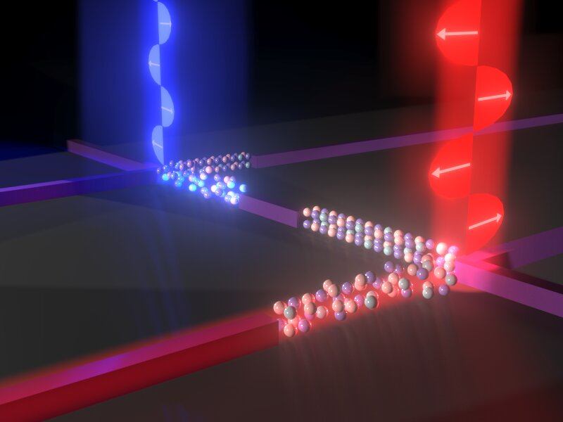
Playing with sharpness and blur does not only allow visual art impressive design possibilities. Sharp contours are also desirable when it comes to creating defined structures for semiconductor technology on very small length scales. However, diffraction of light at very small structures causes clear patterns to soften, which always happens when the scales are in the range of the optical wavelength and thus on the nanoscale.
These diffraction effects dictate the minimum resolution that can be achieved when exposed to a given wavelength or color of light. To achieve very fine nanostructures or very densely packed patterns, really hard light would be ideal. Especially since light affects not only the contours but also the properties of the exposed materials, such as in photolithography, an important method for manufacturing semiconductor devices.
The importance of coating
To create nanopatterns, photoresists are used in semiconductor technology. The solubility of photoresists depends on how they are exposed: There are resists that cure or chemically crosslink upon exposure, and there are resists that soften when exposed to the light of a certain wavelength. Curing coatings are suitable for protecting materials, while softening coatings are used, for example, to define areas where further processing steps are to take place.
The sophisticated sequence of exposures with both types of photoresists is the basis for producing nanostructures that process electrical or optical signals and can be used as integrated building blocks (chips) for electronics and optics. For so-called integrated optics, i.e., optics on a chip basis, scientists usually aim for nanostructures that are smaller than one micrometer. For comparison, hair has a diameter of about 50 micrometers.
Light can be introduced into very small nanostructures with the help of so-called waveguides. This makes circuits possible in which light particles, called photons, act instead of electrons.
Advantage of photonic computers: Light instead of electrons
Since photons move at the speed of light in a vacuum, they always beat out electrons, which are much heavier particles.
Photonic circuits are interesting for all applications that require data to be processed very quickly and without consuming large amounts of energy. This is because light particles work in them instead of electrons. This opens the door to completely new optical computer architectures that do not work like traditional electronic computers but are modeled on the way the human brain works.
Modeled on the brain
The focus is on the development and improvement of these computing architectures. Neuromorphic computers inspired by the construction and operation of the human brain are important for providing hardware for artificial intelligence (AI). AI applications have already arrived in many areas of our everyday lives. For example, they help with speech recognition, encrypt data on smartphones, support search functions, are used for pattern recognition on the Internet, and are essential for safety in autonomous driving.
All these applications pose enormous challenges for conventional electronic computers, because data storage and processing are carried out separately in them. This type of electronic architecture makes it necessary to exchange data continuously via special systems known as bus systems, which leads to sequential clocking and limits data throughput.
Analog computing
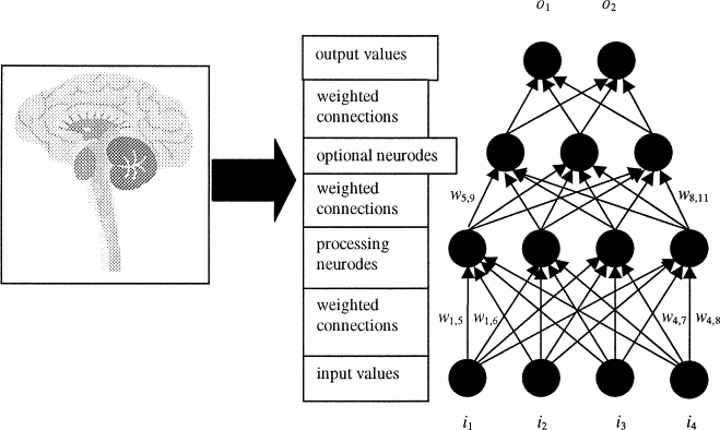
The human brain handles data completely differently: They are processed locally with very high parallelism, and processing is often analog, i.e., continuous, rather than digital, i.e., in steps. This is important for all computational operations required in AI. “Photonic neuromorphic computing” promises to meet these high demands.
Photonic neuromorphic computers use light to perform addition and multiplication as elementary mathematical computational operations. The actual computational task is translated into the encoding of the numbers to be computed together as well as the measurement of the result. Photonic neuromorphic computers can do this in a single step because light particles, unlike electrons, have many degrees of freedom that allow for inherent, simultaneous data processing—this is the special charm of optical computing methods.
How photonic chips calculate
In electronic systems, it is necessary to perform many individual operations one after the other. For data transmission using optical fibers, for example, the wavelength of light is exploited so that data can be exchanged in many colors simultaneously over the same optical fiber.
Faster through parallel processing
This principle can also be used for photonic computers: Different computing operations are encoded on different colors and performed in parallel in the same optical computing system. Parallel processing offers enormous speed increases due to increased clock frequency; the calculations are performed at the speed of light, as it were. Photonic computers can not only compute much faster than electronic systems, but they can also scale in a dimension that is fundamentally unavailable to traditional computers.
Thanks to advances in materials science and integrated optics, photonic circuits can now be designed and simulated on the computer and then manufactured in factories. Fortunately, silicon can be used as a waveguide material, which is also highly compatible with the methods used in the semiconductor industry.
With matrices and vectors
The provision of all these capacities makes it possible to combine individual components into large-scale systems. For optical computing, this means: Small circuits are interconnected to form powerful arithmetic units that perform many multiplications and additions in parallel. This is done with the aid of arithmetic grids or matrices. The inputs of the numbers to be multiplied are available in parallel as vectors.
Based on these, the photonic chips perform matrix-vector calculations using light, with very high data throughput and very low energy consumption. Synthetic structures that mimic nerve cell networks are already being used today in artificial intelligence for cognitive processes. Matrix-vector multiplications are central computations in these neural networks. However, they have to be performed repeatedly, which takes a lot of time and energy.
To save time and energy, scientists try to have the central computational steps performed by special accelerator systems that are optimized for this kind of computational operation and can make them efficiently available for further computations. This is where photonic hardware accelerators come into play: they allow very fast data processing and provide a very large computing capacity in the long term.
Hybrid computing with electrons and light
Photonic computers are very well suited for special operations, while other operations can be better mapped in electronic hardware. The ideal would be “hybrid computers” that work electronically and at the same time contain photonic accelerators. So far, it is still difficult to integrate photonic accelerators into existing electronic computing systems. However, these approaches are attractive models for future high-performance computers that physicists are exploring to satisfy the computational appetite of new AI applications, even in the long term.
Where photonic modules have an advantage
The very high processing speeds make photonic computing modules interesting, for example, for object recognition in autonomous driving, an essential safety requirement. For this purpose, camera and sensor systems record the environment, and the computer must interpret the data so that it can react dynamically to what is happening on the road. AI processes, especially neural networks, are a central component of this.
How fast the overall system reacts is determined by the computing time of the system components: The faster the object detection, the faster the vehicle can be corrected; the accelerator systems thus directly influence the safety of the overall system.
Other interesting applications include training neural networks, which is very time and energy-consuming. Photonic matrix-vector multipliers can be used for this purpose. They offer the advantage of high data throughput, they can be efficiently adapted to different requirements, and they contribute significantly to a reduction in energy consumption.
Phase change as a chip designer
Photonic computers can also be reprogrammed in a variety of ways. One elegant solution is via phase-change materials, such as those used on rewritable DVDs. If these materials exist as hard crystals, they are metal-like. If the crystal structure is disordered or amorphous, the materials are glass-like and transparent. Both states can be very accurately adjusted by exposure to short laser pulses.
The change in material state is used as a basic principle for optical data storage on DVDs, for which the multiplicands of the material property are encoded: Metal-like, hard crystal states represent a logical zero, and glass-like, soft crystal states represent a logical one. Once set, the states are maintained over very long periods of time, up to decades, without the need for external energy input.
Last but not least, it is attractive for practical applications that even very small structures of a phase change material have very large effects on the light via the waveguide used. This allows scientists to reduce the size of the devices and effectively use the space on a chip.
The softness and hardness of light outline a fascinating field of tension: on the one hand, the precise formation of structures with the help of the properties of light, and on the other hand, the adjustment of the degree of hardness of materials through light modifications. Skillful exploitation of this interplay makes it possible to design new lithography processes and new optical methods for data processing.
The transition regions between the two extremes are particularly exciting, such as mixed states of phase change materials that contain both ordered crystalline and disordered components. Equipped with this toolbox, it is then certainly possible to solve even the hardest problems of computer architecture design.